Offshore advanced chip packaging could introduce hidden dependencies, expose sensitive design, and limit the United States’ development of advanced artificial intelligence (AI), high-performance chips (HPC), and defense systems.
To make a chip that can power an AI server, you need three processes:
Over the last two administrations, semiconductor independence has become a national priority, backed by the CHIPS and Science Act. Most funding so far has focused on early-stage manufacturing, allowing the U.S. to complete step one. While the U.S. retains some wafer-testing capabilities, much of steps two and three still occur overseas, leaving the country short of true “chip independence.”
Historically, U.S. chipmakers treated packaging as a back-end step, moving it overseas to cut costs. Today, advanced packaging directly shapes chip performance, and reshoring that expertise is critical to securing the United States’ supply chain and sustaining innovation.
“You can have a fantastic wafer, but without access to packaging innovation, you’re not going to be developing the systems that you really need,” Arizona State University (ASU) Professor Christopher Bailey said. “Having access to an advanced packaging ecosystem is going to be very important for U.S. innovation,” referring to next-generation AI and HPC systems that rely on complex packaging architectures.
Much of the industry’s packaging capacity is concentrated in Taiwan, South Korea, and increasingly China, where outsourced semiconductor assembly and test providers (OSATs) dominate the market, according to Bailey.
“If you keep advanced packaging outside North America, it’s going to result in strategic dependency on what’s happening in those countries,” he said.
For decades, Moore’s Law — doubling the number of transistors on a single chip — delivered predictable performance gains, keeping packaging largely an afterthought. As those gains plateaued, the industry turned to “More than Moore,” combining multiple chips into a single package.
“We can go beyond Moore now,” Bailey said. “Moving away from what we would have called a system on a chip, we’re now looking at systems in a package.”
Today, design choices extend beyond the wafer as performance is increasingly defined at the system level. “The idea of designing chips on wafers, and then essentially throwing those over the wall and saying, ‘well, packaging can get on with it,’ as a low-risk, commodity service no longer applies. Packaging design and chip design, chiplet design, are very much integrated now in terms of the systems that they will support,” he said. “It is now a core part of the system design.”
This shift opens the door to chiplets — smaller, specialized chips — and heterogeneous integration, which combines these chiplets with other components into a single package for greater performance and flexibility, using advanced packaging methods such as fan-out or 2.5D and 3D stacking.
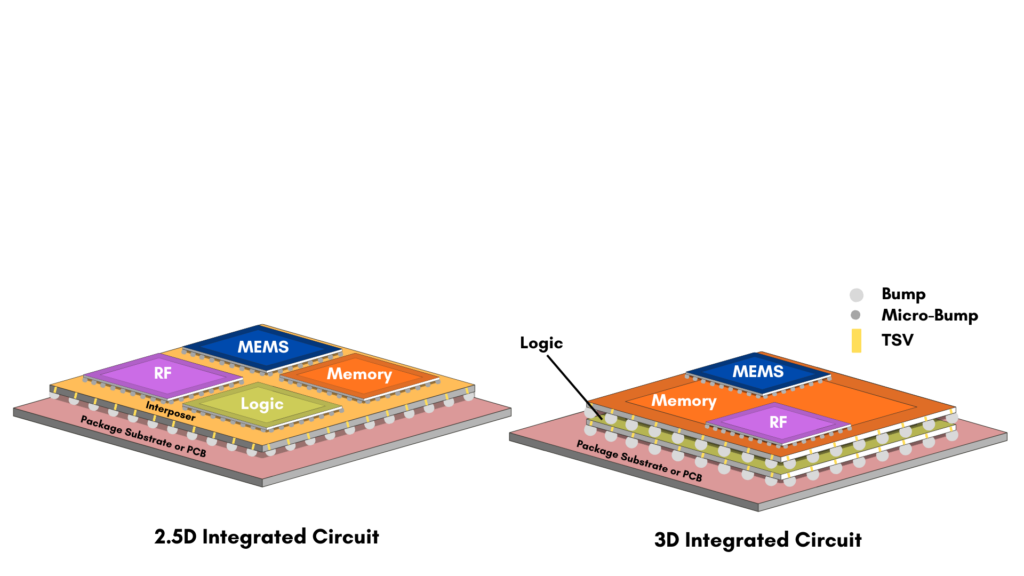
2.5D versus 3D designs. Graphic by Sukhman Sahota
Moving towards heterogeneous integration has brought chip design and packaging closer together, especially in chiplet-based systems. The packaging is not just protection; it links the chips together and directly influences performance, power delivery, and heat management. “It’s much more of a system design than a chip design approach,” he said, highlighting that chips and package design go hand in hand.
When chips fabricated in the U.S. are sent abroad for packaging, the handoff requires sharing design rules, manufacturing data, and often sensitive intellectual property with foreign partners. That could enable foreign partners to become more competitive. Enabling advanced packaging in the US is critical, given the rapid pace of innovation in advanced AI. “It’s really about protecting your ideas,” Bailey said. “Packaging is the key chokepoint here. The system’s innovation, whether it’s in aerospace, automotive, AI, or HPC, comes from advanced packaging.”
Export controls on critical semiconductor resources heighten the risk of relying on overseas packaging, as well. “Advanced packaging is the design of these packages, but it relies on the equipment. It relies on the materials, and some countries would restrict their materials from being used in defense systems — for example, Japan,” he said.
In 2023, Japan began requiring government approval to prevent key semiconductor resources from being used for military purposes.
The U.S. is reshoring its packaging supply chain, with the CHIPS and Science Act pledging $3 billion to boost domestic advanced packaging through research and development, pilot facilities, and workforce development. And since going into action, Arizona is emerging as one of the U.S. hubs for advanced packaging, with TSMC, Intel, and Amkor expanding in the state.
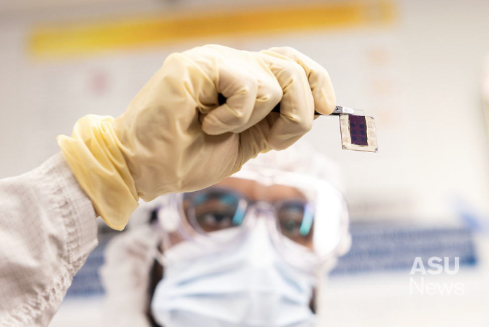
ASU drives a CHIPS Act-funded facility for advanced packaging and prototyping, supporting U.S. semiconductor research and supply chain. The university converted a former Motorola fab into its MacroTechnology Works facility, which, in partnership with DECA Technologies, will soon go live with a full 300mm fan-out wafer prototype.
As the industry continues to invest in research and fabrication, cultivating the next-generation workforce remains a bottleneck to that growth. Packaging is highly multidisciplinary, spanning materials, electrical, thermal, and manufacturing expertise. “We have good experienced folks in these areas, but for the next generation of technicians and engineers, the big thing now will be bringing that workforce through.”
Bailey said years of offshoring the advanced packaging step made it seem like a commoditized function that would always be done abroad. That assumption is now being challenged.
Across the country, federal CHIPS Act funding and new private-sector investments are aimed at rebuilding domestic packaging capacity. Major players, including TSMC, Intel, Samsung, and Amkor have announced or expanded U.S.-based advanced packaging fabrication, further signaling that the back end of chipmaking is no longer an afterthought.
At ASU, that shift has translated into graduate-level coursework and a new micro-credential aimed at pulling engineers from adjacent sectors into semiconductor packaging. The effort reflects a broader push to rebuild domestic expertise across the entire chip supply chain.
Bailey notes that the U.S. advanced packaging investment relies on more than just friend-shoring, but a strong ecosystem. “It’s the industry, the academia, the research institute — the golden triangle all working together,” Bailey said. Workforce, infrastructure, and research support drive where companies choose to invest, making these factors critical to the country’s growth.
Advanced packaging is a critical step in chip manufacturing; it drives chip performance for AI and HPCs and is now a core competitive advantage. Offshore packaging can lead to hidden dependencies, expose intellectual property, and slow the deployment of critical systems — risks that leaders often underestimate. U.S. efforts, supported by the CHIPS Act, are reshoring advanced packaging capabilities, with Arizona emerging as a key hub through investments from TSMC, Intel, Amkor, and research institutions like ASU’s MacroTechnology Works.
A major challenge remains in developing the next-generation workforce. Building expertise across materials, electrical, thermal, and manufacturing disciplines is essential to sustain domestic innovation and secure the semiconductor supply chain.